发布日期:2025/07/04来源:

In February 2025, Hangzhou GAREN Semiconductor Co., Ltd. (hereinafter referred to as "GARENSEMI") achieved a new breakthrough in the crystal growth and processing technology of gallium oxide, successfully preparing a 6-inch oblique cut gallium oxide substrate. The primary surface of the substrate is the (100) plane, tilted 4° along the [00-1] direction.

Figure 1. 6-inch off-cut gallium oxide (β-Ga₂O₃) substrate developed by GARENSEMI.
Here are the characterization results. In terms of substrate quality, the XRD FWHM (full width at half maximum) is less than 90 arcsec, reaching internationally leading standards. Regarding surface morphology, distinct step-terrace structures have formed, facilitating step-flow epitaxial growth. In terms of surface geometry parameters, the substrate exhibits a warp of 14.7 μm, a bow of 5.7 μm, and a total thickness variation (TTV) of 5.7 μm, meeting wafer-level specifications and matching the performance of silicon carbide (SiC) substrates of the same size.
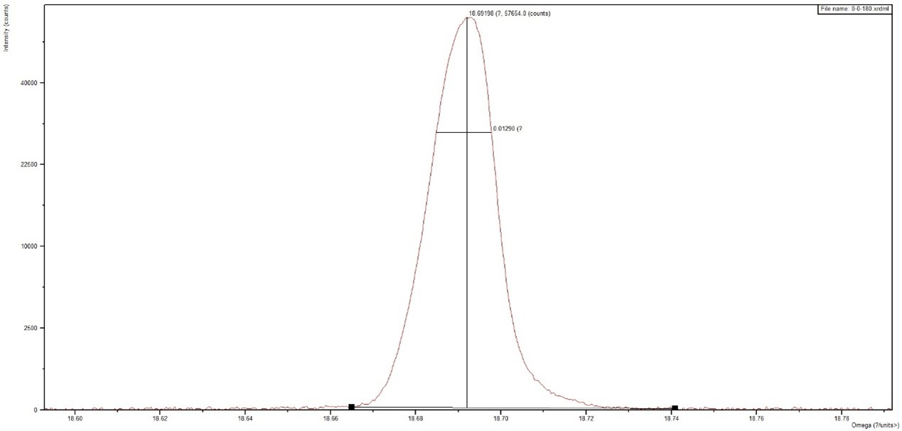
Figure 2. XRD Characterization Data

Figure 3. Surface Roughness Characterization

Figure 4. Surface Geometry Parameter Test Results
Significance of Off-Cut Gallium Oxide Substrates
Conventional (100) on-axis gallium oxide substrates typically induce an island growth mode in epitaxial films. In this mode, lattice-mismatch-induced dislocations accumulate within islands, and small misorientation angles between islands lead to high-density dislocation boundaries upon coalescence, while also increasing surface roughness. Therefore, avoiding island growth is crucial for high-quality epitaxy.
In contrast, (100) off-cut substrates feature a terraced surface, promoting step-flow growth where adatoms preferentially incorporate at step edges. This growth mode suppresses defect formation and maintains smooth surface morphology, closely resembling the substrate's original low roughness.
Furthermore, based on our prior findings, an off-cut along the [00-1] direction exposes (-201) step facets, which additionally inhibit the formation of twin defects.
Notably, researchers from Germany’s Leibniz Institute reported successful fabrication of vertical FinFET devices on 4° off-cut (100) β-Ga2O3 substrates, achieving an average breakdown field strength of 2.7 MV/cm (Kornelius Tetzner et al., Jpn. J. Appl. Phys. 62 SF1010, 2023). Currently, GARENSEMI has entered a global strategic partnership with NextGO Epi, a spin-off from the Leibniz Institute for Crystal Growth (IKZ). Leveraging combined technical strengths, the collaboration aims to advance the R&D and industrialization of gallium oxide semiconductors, injecting new momentum into the global semiconductor industry.
Challenges in Fabricating Off-Cut Gallium Oxide Substrates
While off-cut gallium oxide (β-Ga2O3) substrates offer significant advantages, achieving large-scale industrial production requires overcoming substantial technical hurdles—particularly in manufacturing large-diameter off-cut substrates. Compared to small-sized counterparts, the difficulty escalates exponentially due to two primary challenges:
(1) Growth of Large-Diameter, Thick Single-Crystal Boules
Gallium oxide exhibits strong anisotropic growth, typically restricting boule primary surfaces to low-index crystallographic planes. The (100) plane, with its low surface energy, is the most stable and cost-effective choice, making it ideal for industrialization. However, producing off-cut substrates—especially large-sized ones—demands stringent control over boule dimensions. For instance, fabricating a 6-inch off-cut substrate requires a boule with a diameter more than 6 inches and a thickness more than 11.5 mm. Growing such large, thick single crystals while maintaining homogeneity and minimizing defects (e.g., cracks, inclusions) poses the first major challenge.
(2) Cleavage Cracking and Poor Surface Geometry in Large Substrates
Gallium oxide has two cleavage planes—(100) and (001)—making it prone to cracking during processing. Moreover, as substrate size increases, achieving flatness becomes exponentially harder.

Figure 5 Schematic diagram: requirements for ingot thickness at different angles of oblique cutting
To address these challenges, the R&D team at GARENSEMI has conducted systematic research and made targeted breakthroughs. In crystal growth, the team upgraded the thermal field design and optimized process parameters for the casting method, successfully producing 6-inch gallium oxide boules with thickness exceeding 20 mm. For substrate processing, the team implemented equipment modifications and comprehensive process optimizations, achieving high-quality 6-inch off-cut substrates with surface geometry parameters meeting wafer-level standards.

官方公众号 企微客服
Copyright © 杭州镓仁半导体有限公司 2022-2023 All Rights Reserved 浙ICP备2022037154号


 技术支持
技术支持 在线咨询
在线咨询  电话联系
电话联系