
发布日期:2025/03/07来源:

In March 5, 2025, Hangzhou Garen Semiconductor Co., Ltd. (hereafter as ‘Garen’) unveiled the world’s first 8-inch β-Ga2O3 single crystal. Using the fully independent and innovative casting method, Garen has successfully grown an 8-inch β-Ga2O3 single crystal, and is capable of fabricating corresponding substrates. This breakthrough establishes Garen as the world’s first company to master the growth of 8-inch β-Ga2O3 single crystals, breaking the world record for the diameter of β-Ga2O3 single crystal and setting a milestone by scaling up crystal diameters from 2-inch to 8-inch within one year per generation increment.
China’s β-Ga2O3 industry taking the lead in entering the 8-inch era has profound industrial significance:
First, the 8-inch β-Ga2O3 substrate is fully compatible with the existing 8-inch silicon production lines, significantly accelerating the progress of its industrialization.
Second, β-Ga2O3 substrate with larger diameter can remarkably improve its utilization with lower production costs and higher efficiency.

Figure 1. Garen’s 8-inch β-Ga2O3 single crystal

Figure 2. The rapid advancement of the diameter of β-Ga2O3 single crystal by Garen
**Introduction to β-Ga2O3**
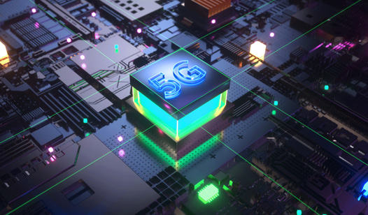
Semiconductor materials serve as the foundation for modern information technology and electronic information industry, acting as a key indicator of the comprehensive national strength. The evolution of semiconductor industry has progressed through the first-generation materials represented by silicon (Si) and germanium (Ge), the second-generation compound semiconductors such as gallium arsenide (GaAs) and indium phosphide (InP), and the third-generation wide bandgap semiconductors exemplified by silicon carbide (SiC) and gallium nitride (GaN). In recent years, with the rapid development of new energy, photovoltaic power generation, radar detection, and 5G mobile communications, ultra-wide bandgap semiconductor materials with wider bandgap and higher breakdown field—notably β-Ga2O3—have attracted widespread attention.
1. Outstanding physical properties of β-Ga2O3
β-Ga2O3 has a bandgap of about 4.8 eV and a breakdown electric field of 8 MV/cm, which is much higher than Si(1.1 eV, 0.3 MV/cm), SiC(3.3eV, 2.5 MV/cm), GaN(3.4 eV, 3.3 MV/cm) and other materials. Power devices fabricated from β-Ga2O3 can operate at high voltage and power.
Furthermore, β-Ga2O3 holds a Baliga’s figure of merit approximately 10 times that of SiC and 4 times that of GaN, enabling devices with lower on-resistance and higher power conversion efficiency.
With a narrow absorption edge (260 nm) and minimal impact of carrier concentration on UV transmittance, β-Ga2O3 demonstrates exceptional advantages in deep-ultraviolet (DUV) optoelectronic devices.
Moreover, β-Ga2O3 crystals have excellent thermal and chemical stability.
Leveraging the aforementioned outstanding physical properties, β-Ga2O3 is promising in high-voltage power devices and DUV optoelectronic applications.

Figure 3. Physical properties of β-Ga2O3 and the benchmark plot of β-Ga2O3 power transistors. (Ref: S. J. Pearton, et al., Appl. Phys. Rev., 5, 2018, 011301;A. J. Green, et al., APL Mater., 10, 2022, 029201)
2. Great application potential of β-Ga2O3
First, β-Ga2O3 holds great potential for power devices, particularly for medium-voltage, high-voltage, and ultra-high-voltage power devices operating at above 650 V, such as fast-charging systems for electrical vehicles (EVs), industrial power supplies, and grid-level high-voltage modules.
Second, β-Ga2O3 can serve as substrate for high-power radio frequency devices, such as communication base stations and radar systems.
Third, the excellent optical-electrical properties of β-Ga2O3 promises its application in solar-blind detection and radiation sensing technologies.
Our life will be radically transformed once β-Ga2O3 is widely adopted.
For example, β-Ga2O3 power devices could elevate onboard electrical systems of EVs to 1,200 V or higher, potentially reducing charging time to 1/4 of current levels and enabling minute-level fast charging.
Furthermore, while SiC can reduces energy losses by ~70% compared to Si, β-Ga2O3 promises an additional 80% reduction over SiC. Consequently, the twin goals of carbon peak and carbon neutrality will be benefited from the application of β-Ga2O3.
3. Advantages of β-Ga2O3 in large-scale industrialization
First, the feasibility of growing large-size β-Ga2O3 single crystal facilitates the industrialization of β-Ga2O3. Similar to traditional semiconductor materials like Si, β-Ga2O3 single crystals can be grown via melt growth methods, making it the only ultra-wide bandgap semiconductor crystal producible through atmospheric-pressure melt growth for large-scale fabrication. Compared to vapor-phase growth, growing from melt ensures larger crystal sizes, higher quality, faster growth rates, lower costs, and mass-production scalability.
Second, the high efficiency of processing also facilitates the industrialization of β-Ga2O3. The hardness of β-Ga2O3 (6) is close to Si (6.5), which is much lower than SiC (9.2), reducing the difficulties in processing. For example, it takes only 20 hours to slice an 8-inch β-Ga2O3 substrate, which is 10 times lower than the 200 hours for one 8-inch SiC substrate. Besides, existing silicon-based cutting, grinding, and polishing equipment and technologies can be directly adapted for β-Ga2O3, slashing R&D cycles and costs while accelerating industrialization.
**Introduction to the casting method**
1.Origin and advantages of the casting method
The casting method, a novel melt-growth technology for producing β-Ga2O3 single crystals, was independently developed by the research team led by Yang Deren, the academician of the Chinese academy of sciences from Zhejiang university. This method offers the following key advantages:
Cost-effectiveness: The usage and loss of precious metal iridium is significantly reduced compared to other conventional techniques, leading to lower production costs.
High efficiency: The casting method grows thick crystals (20 mm) at high rates (~100 mm/h), enabling high wafer yield per ingot and streamlined production.
Simplicity and scalability: the casting methods features a short process flow, easy scalability to larger dimensions, and precise controllability.
2. Evolution of Garen’s growth of β-Ga2O3 using the casting method
Since its founding in 2022, Garen has rapidly scaled up crystal dimensions within one year per generation increment, showcasing its autonomous innovation capabilities. In May 2020, 2-inch β-Ga2O3 single crystal was successfully developed; in May 2023, 4-inch β-Ga2O3 single crystal was demonstrated; in February 2024, 6-inch β-Ga2O3 single crystal was introduced. And in February 2025, Garen pioneered the world’s first 8-inch β-Ga2O3 single crystal.
3. The industrialization of the casting method and its high product quality
Garen kept on advancing the casting method toward large-scale industrialization, delivering high-quality, large-diameter β-Ga2O3 single-crystal substrates to downstream clients. Currently, 6-inch β-Ga2O3 substrates have entered commercial production and are being shipped to customers.


Figure 4. Third party test report of Garen’s β-Ga2O3 single crystal substrate products
(Left: results of electrical performance. The conductive crystal has a resistivity of 25 mΩ·cm and a carrier concentration of 2.9×1018cm-1. the UID crystal has a resistivity of 664 mΩ·cm and a carrier concentration of 6.9×1016cm-1; Right: results of crystal quality. XRD half-height full width (FWHM) is 19 arcsec.)
**The vertical Bridgeman growth system self-developed by Garen for β-Ga2O3 is now fully open to sales**
Garen not only provides β-Ga2O3 single crystal substrates, but also fully opens the sale of vertical Bridgeman crystal growth equipment and customized process packages for β-Ga2O3.
In September 2024, Garen launched its first self-developed vertical Bridgeman growth system for β-Ga2O3. This system is designed to maintain the high-temperature and high-oxygen environments required for β-Ga2O3 growth, with the capability of fully automated crystal growth. While manual intervention is minimized, the production efficiency and crystal quality are quite remarkable.
The equipment can obtain a variety of large-size single crystals with different crystal planes through process control, and support the upgrading to larger-size single crystals to meet the needs of universities, research institutes, and corporate customers for scientific research and production of β-Ga2O3 crystal growth. This VB method β-Ga2O3 crystal growth equipment and its process package have been fully opened for sale.
**Company overview**
Founded in September 2022 and located in Xiaoshan District, Hangzhou, Hangzhou Garen Semiconductor Co., Ltd. is a high-tech enterprise specialized in R&D, production, and sales of wide-bandgap semiconductor material β-Ga2O3 and related equipment.
Relying on the State Key Laboratory of Silicon and Advanced Semiconductor Materials of Zhejiang university and the ZJU-Hangzhou Global Scientific and Technological Innovation Center, Garen has formed a R&D and production team with Yang Deren, the academician of Chinese Academy of Sciences, as the chief consultant. The R&D team of Garen developed the novel casting method and achieved the growth of 8-inch β-Ga2O3 single crystal. Garen is the world’s first company capable of growing 8-inch β-Ga2O3 single crystal, positioning itself in the international leading level. Garen has also achieved the 3-inch (010)-oriented substrates, which is currently the largest reported across the world. Garen has independently developed the vertical Bridgeman growth system for growing β-Ga2O3 at high temperature and high-oxygen environments. This system is capable of fully automated crystal growth, minimizing manual intervention while improving efficiency and quality.
Garen has been certified as the national technology-oriented SME, Zhejiang’s “Specialized & Innovative” SME, Zhejiang’s innovative SME, Zhejiang’s science and technology SME, Hangzhou’s enterprise high-tech research and development center. Garen has filed 50+ domestic and international patents.
Garen’s products include β-Ga2O3 substrates of multiple sizes, crystal orientations and resistance, customized β-Ga2O3 seed crystals and et al. Garen’s products are mainly applied in power electronics for national grid systems, electrical vehicles, rail transit, 5G communications and et al. After years of research, Garen can deliver fully IP-independent substrates, with full control over equipment design, thermal field optimization, crystal growth, and wafer processing.
**Contact us**
For detailed information about Garen and our products, visit http://garen.cc/ or contact:
Mr. Jiang: +86 15918719807 | jiangjiwei@garen.cc
Mr. Xia: +86 19011278792 | xianing@garen.cc
Hangzhou Gallium Semiconductors Co., Ltd. looks forward to collaborating with global partners to shape the future of semiconductor technology


官方公众号 企微客服
Copyright © 杭州镓仁半导体有限公司 2022-2023 All Rights Reserved 浙ICP备2022037154号


 技术支持
技术支持 在线咨询
在线咨询  电话联系
电话联系